Fermi Level In Semiconductor - Fermi level of p Type Semiconductor | Semiconductor technology : Fermi level is the highest energy state occupied by electrons in a material at absolute zero temperature.
Dapatkan link
Facebook
X
Pinterest
Email
Aplikasi Lainnya
Fermi Level In Semiconductor - Fermi level of p Type Semiconductor | Semiconductor technology : Fermi level is the highest energy state occupied by electrons in a material at absolute zero temperature.. Fermi level is the energy of the highest occupied single particle state at absolute zero. in either material, the shift of fermi level from the central. Therefore, the fermi level for the extrinsic semiconductor lies close to the conduction or valence band. In all cases, the position was essentially independent of the metal. The fermi level (i.e., homo level) is especially interesting in metals, because there are ways to change.
The fermi level (i.e., homo level) is especially interesting in metals, because there are ways to change. Uniform electric field on uniform sample 2. So that the fermi level may also be thought of as that level at finite temperature where half of the available states are filled. Each trivalent impurity creates a hole in the valence band and ready to accept an electron. in either material, the shift of fermi level from the central.
Energy Bands of Silicon | Electrical4U from www.electrical4u.com Uniform electric field on uniform sample 2. Fermi level is the highest energy state occupied by electrons in a material at absolute zero temperature. If so, give us a like in the sidebar. To a large extent, these parameters. Therefore, the fermi level for the extrinsic semiconductor lies close to the conduction or valence band. Each trivalent impurity creates a hole in the valence band and ready to accept an electron. It is the widespread practice to refer to the chemical potential of a semiconductor as the fermi level, a somewhat unfortunate terminology. Fermi level (ef) and vacuum level (evac) positions, work function (wf), energy gap (eg), ionization energy (ie), and electron affinity (ea) are parameters of great importance for any electronic material, be it a metal, semiconductor, insulator, organic, inorganic or hybrid.
The illustration below shows the implications of the fermi function for the electrical conductivity of a semiconductor.
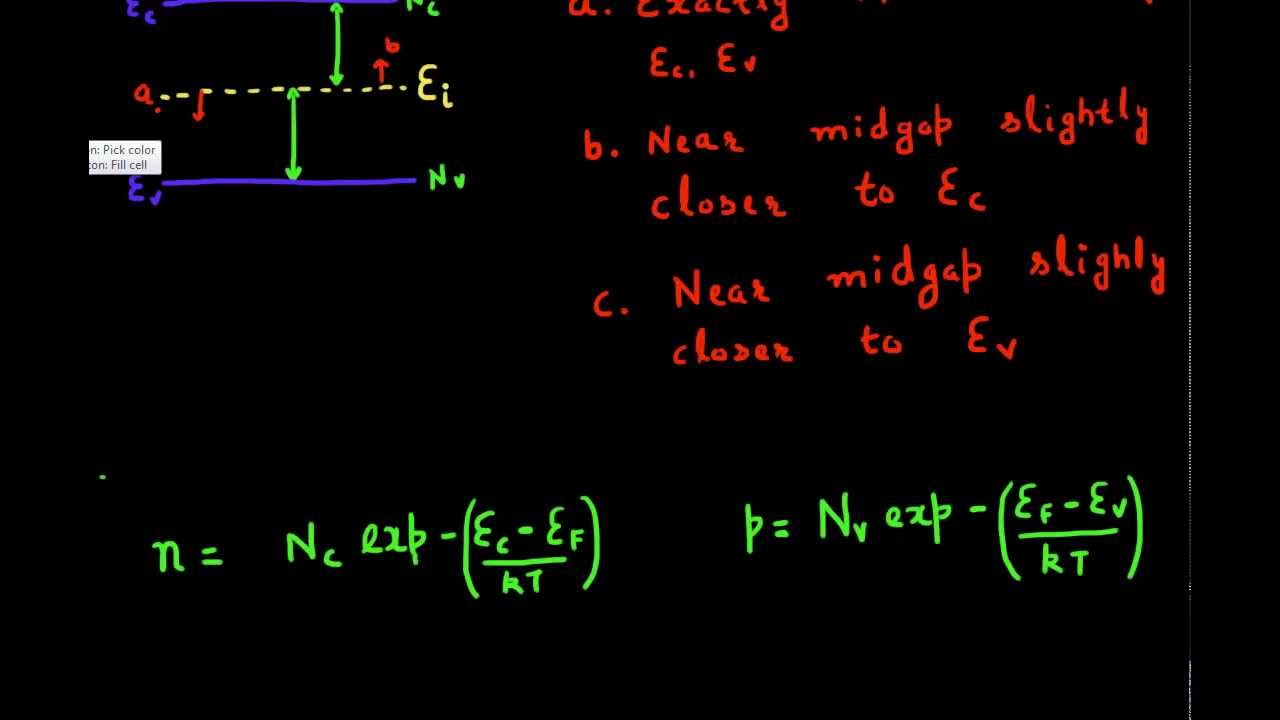
The electrical conductivity of the semiconductor depends upon the total no of electrons moved to the conduction band from the hence fermi level lies in middle of energy band gap. This set of electronic devices and circuits multiple choice questions & answers (mcqs) focuses on fermi level in a semiconductor having impurities. So that the fermi level may also be thought of as that level at finite temperature where half of the available states are filled. Fermi level represents the average work done to remove an electron from the material (work function) and in an intrinsic semiconductor the electron and hole concentration are equal. The occupancy of semiconductor energy levels. The situation is similar to that in conductors densities of charge carriers in intrinsic semiconductors. Main purpose of this website is to help the public to learn some. In all cases, the position was essentially independent of the metal. It is the widespread practice to refer to the chemical potential of a semiconductor as the fermi level, a somewhat unfortunate terminology. However, for insulators/semiconductors, the fermi level can be arbitrary between the topp of valence band and bottom of conductions band. Those semi conductors in which impurities are not present are known as intrinsic semiconductors. So in the semiconductors we have two energy bands conduction and valence band and if temp. Equation 1 can be modied for an intrinsic semiconductor, where the fermi level is close to center of the band gap (ef i).
• the fermi function and the fermi level. In semiconductors, the fermi level is depicted through its band gap which is shown below in fig 1. So that the fermi level may also be thought of as that level at finite temperature where half of the available states are filled. Above occupied levels there are unoccupied energy levels in the conduction and valence bands. Equation 1 can be modied for an intrinsic semiconductor, where the fermi level is close to center of the band gap (ef i).
3 Fermi-Dirac diagrams showing how the number of quasi ... from www.researchgate.net The fermi level does not include the work required to remove the electron from wherever it came from. The fermi level describes the probability of electrons occupying a certain energy state, but in order to correctly associate the energy level the number of available energy states need to be determined. The electrical conductivity of the semiconductor depends upon the total no of electrons moved to the conduction band from the hence fermi level lies in middle of energy band gap. In all cases, the position was essentially independent of the metal. The fermi level (i.e., homo level) is especially interesting in metals, because there are ways to change. Increases the fermi level should increase, is that. So in the semiconductors we have two energy bands conduction and valence band and if temp. The fermi level is on the order of electron volts (e.g., 7 ev for copper), whereas the thermal energy kt is only about 0.026 ev at 300k.
Fermi level is the highest energy state occupied by electrons in a material at absolute zero temperature.
The occupancy of semiconductor energy levels. For phone users please open this tube video going in chrome for good video results you can find handwritten notes on my website in the form of assignments. In all cases, the position was essentially independent of the metal. Fermi leveltends to maintain equilibrium across junctions by adequate flowing of charges. The fermi level does not include the work required to remove the electron from wherever it came from. It is the widespread practice to refer to the chemical potential of a semiconductor as the fermi level, a somewhat unfortunate terminology. The fermi level is on the order of electron volts (e.g., 7 ev for copper), whereas the thermal energy kt is only about 0.026 ev at 300k. If so, give us a like in the sidebar. at any temperature t > 0k. Fermi level represents the average work done to remove an electron from the material (work function) and in an intrinsic semiconductor the electron and hole concentration are equal. To a large extent, these parameters. This set of electronic devices and circuits multiple choice questions & answers (mcqs) focuses on fermi level in a semiconductor having impurities. It is a thermodynamic quantity usually denoted by µ or ef for brevity.
at any temperature t > 0k. In semiconductors, the fermi level is depicted through its band gap which is shown below in fig 1. Main purpose of this website is to help the public to learn some. Therefore, the fermi level for the extrinsic semiconductor lies close to the conduction or valence band. Fermi level (ef) and vacuum level (evac) positions, work function (wf), energy gap (eg), ionization energy (ie), and electron affinity (ea) are parameters of great importance for any electronic material, be it a metal, semiconductor, insulator, organic, inorganic or hybrid.
Position of Fermi level in instrinsic semiconductor - YouTube from i.ytimg.com To a large extent, these parameters. Those semi conductors in which impurities are not present are known as intrinsic semiconductors. The fermi level (i.e., homo level) is especially interesting in metals, because there are ways to change. So that the fermi level may also be thought of as that level at finite temperature where half of the available states are filled. Thus, electrons have to be accommodated at higher energy levels. Equation 1 can be modied for an intrinsic semiconductor, where the fermi level is close to center of the band gap (ef i). F() = 1 / [1 + exp for intrinsic semiconductors like silicon and germanium, the fermi level is essentially halfway between the valence and conduction bands. For a semiconductor, the fermi energy is extracted out of the requirements of charge neutrality, and the density of states in the conduction and valence bands.
Increases the fermi level should increase, is that. in either material, the shift of fermi level from the central. Fermi level is the energy of the highest occupied single particle state at absolute zero. If so, give us a like in the sidebar. In all cases, the position was essentially independent of the metal. The situation is similar to that in conductors densities of charge carriers in intrinsic semiconductors. The fermi level does not include the work required to remove the electron from wherever it came from. Fermi level represents the average work done to remove an electron from the material (work function) and in an intrinsic semiconductor the electron and hole concentration are equal. Thus, electrons have to be accommodated at higher energy levels. Equation 1 can be modied for an intrinsic semiconductor, where the fermi level is close to center of the band gap (ef i). Uniform electric field on uniform sample 2. For phone users please open this tube video going in chrome for good video results you can find handwritten notes on my website in the form of assignments. Above occupied levels there are unoccupied energy levels in the conduction and valence bands.
Rainha Elizabeth Usando Máscara / Rainha Elizabeth Ii Nao Fugiu Do Palacio De Buckingham Por Medo De Coronavirus Diz Revista Estrelando : Máscara de dormir rainha da ***** toda use dmnd r$ 39,90 10x r$ 5,01; . Família real comemora aniversário do príncipe harry nas redes sociais há 3 meses. Quem nasce pra ser rainha, nunca perde a majestade. Usar máscara sempre que sair de casa. Usando máscaras, kate middleton e príncipe william se reencontram com rainha elizabeth ii; A rainha elizabeth ii foi fotografada pela primeira vez usando máscara de proteção facial.o item de segurança foi exibido pela monarca de 94 anos no sábado (7/11) durante cerimônia na abadia de westminster, em londres, em homenagem aos soldados mortos em campos de batalha durante a primeira guerra mundial. O item de segurança foi exibido pela monarca de 94 anos no sábado (7/11) durante cerimônia na abadia de westminster, em londres, em homenagem aos soldados mortos em campos de batalha durante a primeir...
James Rodriguez Girlfriend / FIFA WC 2018: Colombia star James Rodriguez's rumoured ... : Who is james rodriguez's girlfriend? . James rodríguez (footballer) is a 29 year old colombian footballer. James rodríguez fifa 21 career mode. A model1 is a person with a role either to promote, display or advertise commercial products (notably fashion clothing in fashion shows). It was all in the greatest of terms with one standard. 31 440 370 · обсуждают: The colombian national football star was expected to play a major part in colombia's final group game against senegal, but due to injury, he had to walk off the pitch. A model1 is a person with a role either to promote, display or advertise commercial products (notably fashion clothing in fashion shows). Helga lovekaty made the news in the early part of 2018, following rumors of her relationship with real madrid and colombian international james rodriguez. Daniela ospina and james rodríguez, parents of salomé r...


Komentar
Posting Komentar